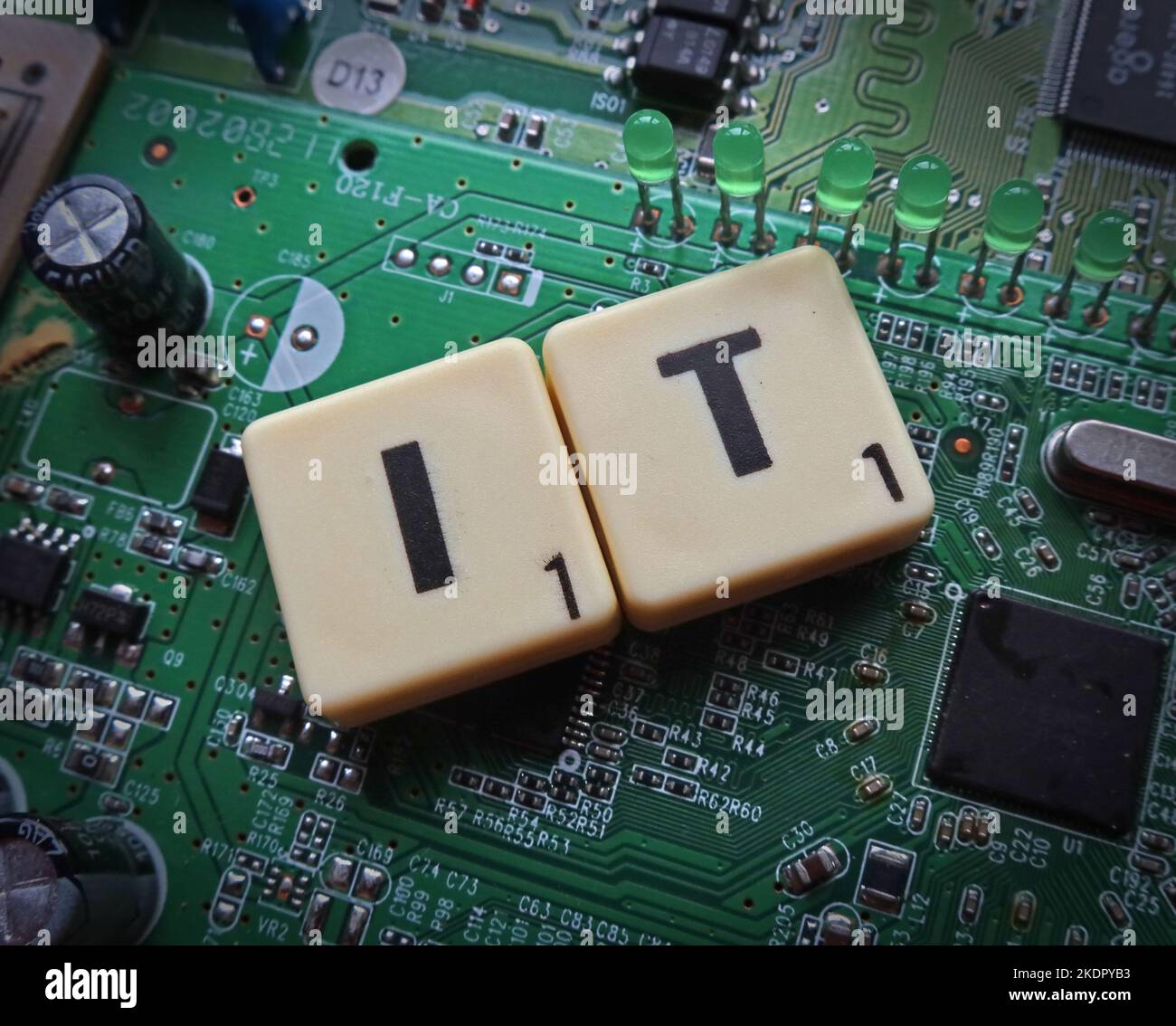
IT - Information Technology - Scrabble letters / word on a electronic PCB
Image details
Contributor:
Tony Smith / Alamy Stock PhotoImage ID:
2KDPYB3File size:
33.1 MB (1 MB Compressed download)Releases:
Model - no | Property - noDo I need a release?Dimensions:
3792 x 3048 px | 32.1 x 25.8 cm | 12.6 x 10.2 inches | 300dpiDate taken:
8 November 2022More information:
A printed circuit board (PCB; also printed wiring board or PWB) is a medium used in electrical and electronic engineering to connect electronic components to one another in a controlled manner. It takes the form of a laminated sandwich structure of conductive and insulating layers: each of the conductive layers is designed with an artwork pattern of traces, planes and other features (similar to wires on a flat surface) etched from one or more sheet layers of copper laminated onto and/or between sheet layers of a non-conductive substrate. Electrical components may be fixed to conductive pads on the outer layers in the shape designed to accept the component's terminals, generally by means of soldering, to both electrically connect and mechanically fasten them to it. Another manufacturing process adds vias: plated-through holes that allow interconnections between layers The Austrian engineer Paul Eisler invented the printed circuit as part of a radio set while working in the UK around 1936. In 1941 a multi-layer printed circuit was used in German magnetic influence naval mines Around 1943 the USA began to use the technology on a large scale to make proximity fuzes for use in World War II. Such fuzes required an electronic circuit that could withstand being fired from a gun, and could be produced in quantity Motorola was an early leader in bringing the process into consumer electronics, announcing in August 1952 the adoption of "plated circuits" in home radios after six years of research and a $1M investment Originally, every electronic component had wire leads, and a PCB had holes drilled for each wire of each component. The component leads were then inserted through the holes and soldered to the copper PCB traces. This method of assembly is called through-hole construction. In 1949, Moe Abramson and Stanislaus F. Danko of the United States Army Signal Corps developed the Auto-Sembly process in which component leads were inserted into a copper foil interconnection